ON FDC5661N
N 通道60 V4.3A(Ta)3V @ 250µA1.6W(Ta)-55°C ~ 150°C(TJ)表面贴装型
比较


¥1.14
价格更新:一个月前博斯克质量保证


Overview
The FDC5614P is MOSFET P-CH 60V 3A SSOT-6, that includes Reel Packaging, they are designed to operate with a FDC5614P_NL Part Aliases, Unit Weight is shown on datasheet note for use in a 0.001270 oz, that offers Mounting Style features such as SMD/SMT, Package Case is designed to work in SSOT-6, as well as the Si Technology, the device can also be used as 1 Channel Number of Channels. In addition, the Configuration is Single Quad Drain, the device is offered in 1 P-Channel Transistor Type, the device has a 1.6 W of Pd Power Dissipation, it has an Maximum Operating Temperature range of + 150 C, it has an Minimum Operating Temperature range of - 55 C, and Fall Time is 10 ns, and the Rise Time is 10 ns, and Vgs Gate Source Voltage is 20 V, and the Id Continuous Drain Current is 3 A, and Vds Drain Source Breakdown Voltage is - 60 V, and the Rds On Drain Source Resistance is 105 mOhms, and Transistor Polarity is P-Channel, and the Typical Turn Off Delay Time is 19 ns, and Typical Turn On Delay Time is 7 ns, and the Forward Transconductance Min is 8 S, and Channel Mode is Enhancement.
FDC5614P-NL with circuit diagram manufactured by FAIRCHILD. The FDC5614P-NL is available in TSOP-6 Package, is part of the IC Chips.
Features
PowerTrench® SeriesBulk Package
MOSFET (Metal Oxide) Technology
60 V Drain to Source Voltage (Vdss)
4.3A (Ta) Current - Continuous Drain (Id) @ 25°C
4.5V, 10V Drive Voltage (Max Rds On, Min Rds On)
47mOhm @ 4.3A, 10V Rds On (Max) @ Id, Vgs
3V @ 250µA Vgs(th) (Max) @ Id
19 nC @ 10 V Gate Charge (Qg) (Max) @ Vgs
±20V Vgs (Max)
763 pF @ 25 V Input Capacitance (Ciss) (Max) @ Vds
1.6W (Ta) Power Dissipation (Max)
Surface Mount Mounting Type
- 起步价为$40,南非、巴西、印度、巴基斯坦、以色列等国家的价格会有所变动,详情请咨询相关客服人员。
- 包裹重量≤0.5kg的基本运费根据时区和国家而定。
- 我们的产品目前使用DHL,顺丰和UPS运输。如果数量少,则选择联邦快递。
- 一旦发货,预期交货时间跟选择的运输方式有所变动。
准备产品

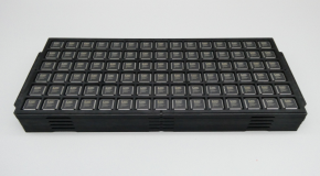
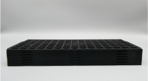
真空包装

防静电袋

单独包装

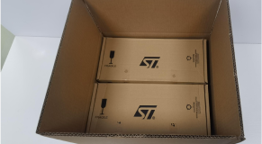
包装盒

条形码运输标签


onsemi
onsemi(前称ON Semiconductor)是一家全球领先的半导体供应商,致力于提供智能电源和传感技术。公司成立于1999年,总部位于美国亚利桑那州斯科茨代尔。onsemi的产品涵盖汽车、工业、电源管理和物联网等领域。
热门零件号
实时新闻
博斯克数字
收入: 85M
2022年的收入为8500万美元,与2021年增长63%。
国家: 105
博斯克服务全球105个国家的客户。
配件发货: 25M+
我们在过去的五年中发货了2.5亿个配件,比前五年增长148%。
制造商: 950
2022年,博斯克从近950个制造商售卖了配件。
热门产品

FDN340P
onsemi
MOSFET P-CH 20V 2A SUPERSOT3

FDMC86139P
onsemi
MOSFET P-CH 100V 4.4A/15A 8MLP

FDN338P
onsemi
MOSFET P-CH 20V 1.6A SUPERSOT3

FDMS86200
onsemi
MOSFET N-CH 150V 9.6A/35A 8PQFN

FDC604P
onsemi
MOSFET P-CH 20V 5.5A SUPERSOT6

FDD2572
onsemi
MOSFET N-CH 150V 4A/29A TO252AA

BSS138LT1G
onsemi
MOSFET N-CH 50V 200MA SOT23-3

FDV301N
onsemi
MOSFET N-CH 25V 220MA SOT23

2N7002LT1G
onsemi
MOSFET N-CH 60V 115MA SOT23-3

FDMA908PZ
onsemi
MOSFET P-CH 12V 12A 6MICROFET


