
ST STF10NK50Z
N 通道500 V9A(Tc)4.5V @ 100µA30W(Tc)-55°C ~ 150°C(TJ)通孔
比较


¥0.93
价格更新:一个月前博斯克质量保证


Overview
The STF10N80K5 is MOSFET N-CH 800V 9A TO-220FP, that includes MDmesh? Series, they are designed to operate with a Tube Packaging, Unit Weight is shown on datasheet note for use in a 0.011640 oz, that offers Mounting Style features such as Through Hole, Package Case is designed to work in TO-220-3 Full Pack, as well as the Si Technology, it has an Operating Temperature range of -55°C ~ 150°C (TJ). In addition, the Mounting Type is Through Hole, the device is offered in 1 Channel Number of Channels, the device has a TO-220FP of Supplier Device Package, and Configuration is Single, and the FET Type is MOSFET N-Channel, Metal Oxide, and Power Max is 30W, and the Transistor Type is 1 N-Channel, and Drain to Source Voltage Vdss is 800V, and the Input Capacitance Ciss Vds is 635pF @ 100V, and FET Feature is Standard, and the Current Continuous Drain Id 25°C is 9A (Tc), and Rds On Max Id Vgs is 600 mOhm @ 4.5A, 10V, and the Vgs th Max Id is 5V @ 100μA, and Gate Charge Qg Vgs is 22nC @ 10V, and the Pd Power Dissipation is 30 W, it has an Maximum Operating Temperature range of + 150 C, it has an Minimum Operating Temperature range of - 55 C, and Fall Time is 14 ns, and the Rise Time is 11 ns, and Vgs Gate Source Voltage is 30 V, and the Id Continuous Drain Current is 9 A, and Vds Drain Source Breakdown Voltage is 800 V, and the Vgs th Gate Source Threshold Voltage is 3 V, and Rds On Drain Source Resistance is 470 mOhms, and the Transistor Polarity is N-Channel, and Typical Turn Off Delay Time is 35 ns, and the Typical Turn On Delay Time is 14.5 ns, and Qg Gate Charge is 22 nC, and the Channel Mode is Enhancement.
The STF10N65K3 is MOSFET N-CH 650V 10A TO-220FP, that includes 35 ns Fall Time, they are designed to operate with a 10 A Id Continuous Drain Current, it has an Maximum Operating Temperature range of + 150 C, it has an Minimum Operating Temperature range of - 55 C, Mounting Style is designed to work in Through Hole, as well as the 1 Channel Number of Channels, the device can also be used as TO-220-3 Package Case. In addition, the Packaging is Tube, the device is offered in 35 W Pd Power Dissipation, the device has a 42 nC of Qg Gate Charge, and Rds On Drain Source Resistance is 750 mOhms, and the Rise Time is 14 ns, and Series is N-channel MDmesh, and the Technology is Si, and Transistor Polarity is N-Channel, and the Transistor Type is 1 N-Channel, and Typical Turn Off Delay Time is 44 ns, and the Typical Turn On Delay Time is 14.5 ns, and Unit Weight is 0.011640 oz, and the Vds Drain Source Breakdown Voltage is 650 V, and Vgs Gate Source Voltage is 30 V.
Features
SuperMESH™ SeriesExtremely high dv/dt capability
100% avalanche tested
Gate charge minimized
Very low intrinsic capacitance
Applications
High level of dv/dt capability for the most demanding applications
- 起步价为$40,南非、巴西、印度、巴基斯坦、以色列等国家的价格会有所变动,详情请咨询相关客服人员。
- 包裹重量≤0.5kg的基本运费根据时区和国家而定。
- 我们的产品目前使用DHL,顺丰和UPS运输。如果数量少,则选择联邦快递。
- 一旦发货,预期交货时间跟选择的运输方式有所变动。
准备产品
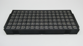
真空包装
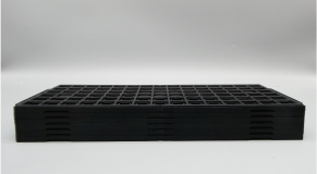
防静电袋
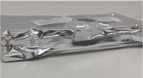
单独包装

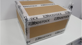
包装盒
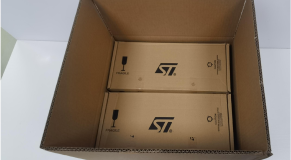
条形码运输标签

STMicroelectronics
STMicroelectronics(ST)是一家领先的半导体公司,成立于1987年,总部位于瑞士日内瓦。公司提供多种半导体解决方案,应用于汽车、工业、个人电子和通信等领域。ST的产品组合包括微控制器、传感器、模拟IC和电源管理芯片等。
热门零件号
实时新闻
博斯克数字
收入: 85M
2022年的收入为8500万美元,与2021年增长63%。
国家: 105
博斯克服务全球105个国家的客户。
配件发货: 25M+
我们在过去的五年中发货了2.5亿个配件,比前五年增长148%。
制造商: 950
2022年,博斯克从近950个制造商售卖了配件。
热门产品

STN3NF06L
STMicroelectronics
MOSFET N-CH 60V 4A SOT223

STF9NK90Z
STMicroelectronics
MOSFET N-CH 900V 8A TO220FP

STP21N65M5
STMicroelectronics
MOSFET N-CH 650V 17A TO220AB

STW3N150
STMicroelectronics
MOSFET N-CH 1500V 2.5A TO247-3

STP7NK80ZFP
STMicroelectronics
MOSFET N-CH 800V 5.2A TO220FP

STW70N60M2
STMicroelectronics
MOSFET N-CH 600V 68A TO247

STD5N52U
STMicroelectronics
MOSFET N-CH 525V 4.4A DPAK

STF6N95K5
STMicroelectronics
MOSFET N-CH 950V 9A TO220FP

STW28N60DM2
STMicroelectronics
MOSFET N-CH 600V 21A TO247

STN1NK80Z
STMicroelectronics
MOSFET N-CH 800V 250MA SOT223


