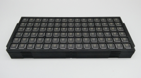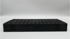
NXP MC68EC060RC75
6806075MHz0°C ~ 70°C(TA)
比较


面议
价格更新:一个月前博斯克质量保证


Overview
The superscalar MC68060 represents a new line of Motorola microprocessor products. The first generation of the M68060 product line consists of the MC68060, MC68LC060, and MC68EC060. All three microprocessors offer superscalar integer performance of over 100 MIPS at 66 MHz. The MC68060 comes fully equipped with both a floating-point unit (FPU) and a memory management unit (MMU) for high-performance embedded control and desktop applications. For cost-sensitive embedded control and desktop applications where an MMU is required, but the additional cost of a FPU is not justified, the MC68LC060 offers high-performance at a low cost. Specifically designed for low-cost embedded control applications, the MC68EC060RC75 eliminates both the FPU and MMU, permitting designers to leverage MC68060 performance while avoiding the cost of unnecessary features. Throughout this product brief, all references to the MC68060 also refer to the MC68LC060 and the MC68EC060, unless otherwise noted.Leveraging many of the same performance enhancements used by RISC designs as well as providing innovative architectural techniques, the MC68060 harnesses new levels of performance for the M68000 family. Incorporating 2.5 million transistors on a single piece of silicon, the MC68060 employs a deep pipeline, dual issue superscalar execution, a branch cache, a high-performance floating-point unit (MC68060 only), eight Kbytes each of on-chip instruction and data caches, and dual on-chip demand paging MMUs (MC68060 and MC68LC060 only). The MC68060 allows simultaneous execution of two integer instructions (or an integer and a float instruction) and one branch instruction during each clock.The MC68060 features a full internal Harvard architecture. The instruction and data caches are designed to support concurrent instruction fetch, operand read and operand write references on every clock. Separate 8-Kbyte instruction and 8-Kbyte data caches can be frozen to prevent allocation over time-critical code or data. The independent nature of the caches allows instruction stream fetches, data-stream fetches, and external accesses to occur simultaneously with instruction execution. The operand data cache is four-way banked to permit simultaneous read and write access each clock.A very high bandwidth internal memory system coupled with the compact nature of the M68000 family code allows the MC68060 to achieve extremely high levels of performance, even when operating from low-cost memory such as a 32-bit wide dynamic random access memory system.Instructions are fetched from the internal cache or external memory by a four-stage instruction fetch pipeline. The MC68060 variable-length instruction system is internally decoded into a fixed-length representation and channeled into an instruction buffer. The instruction buffer acts as a FIFO which provides a decoupling mechanism between the instruction fetch unit and the operand execution units. Fixed format instructions are dispatched to dual fourstage pipelined RISC operand execution engines where they are then executed.The branch cache also plays a major role in achieving the high performance levels of the MC68060. It has been implemented such that most branches are executed in zero cycles. Using a technique known as branch folding, the branch cache allows the instruction fetch pipeline to detect and change the instruction prefetch stream before the change of flow affects the instruction execution engines, minimizing the need for pipeline refill.In addition to substantial cost and performance benefits, the MC68060 also offers advantages in power consumption and power management. The MC68060 automatically minimizes power dissipation by using a fully-static design, dynamic power management, and low-voltage operation. It automatically powers-down internal functional blocks that are not needed on a clock-by-clock basis. Explicitly the MC68060 power consumption can be controlled from the operating system. Although the MC68060 operates at a lower operating voltage, it directly interfaces to both 3-V and 5-V peripherals and logic.Complete code compatibility with the M68000 family allows the designer to draw on existing code and past experience to bring products to market quickly. There is also a broad base of established development tools, including real-time kernels, operating systems, languages, and applications, to assist in product design. The functionality provided by the MC68060 makes it the ideal choice for a range of high-performance embedded applications and computing applications. With M68000 family code compatibility, the MC68060 provides a range of upgrade opportunities to virtually any existing MC68040 application.
Features
M680x0 Series1.6–1.7 Times the MC68040 Performance at the Same Clock Rate with Existing Compliers. 3.2–3.4 Times the Performance of a 25 MHZ MC68040.
Harvard Architecture with Independent, Decoupled Fetch, and Execution Pipelines.
Branch Prediction Logic with a 256-Entry, 4-Way Set-Associative, Virtual-Mapped Branch Cache for Improved Branch Instruction Performance.
A Superscalar Pipeline and Dual Integer Execution Units Achieving Simultaneous, but not Out-of-Order Instruction Execution.
An IEEE Standard, MC68040- and MC68881-/MC68882-Compatible FPU.
Dual 8-Kbyte Caches (Instruction Cache and Data Cache)
A Flexible, High-Bandwidth Synchronous Bus Interface
User Object-Code Compatible with All Earlier M68000 Microprocessors
Applications
Automotive
Advanced driver assistance systems (ADAS)
Industrial
Pro audio, video & signage
Enterprise systems
Enterprise machine
- 起步价为$40,南非、巴西、印度、巴基斯坦、以色列等国家的价格会有所变动,详情请咨询相关客服人员。
- 包裹重量≤0.5kg的基本运费根据时区和国家而定。
- 我们的产品目前使用DHL,顺丰和UPS运输。如果数量少,则选择联邦快递。
- 一旦发货,预期交货时间跟选择的运输方式有所变动。
准备产品

真空包装

防静电袋

单独包装

包装盒

条形码运输标签


NXP USA Inc.
NXP USA Inc.是NXP Semiconductors在美国的子公司,负责设计、研发、制造和销售半导体产品。公司在德克萨斯州奥斯汀和亚利桑那州钱德勒设有晶圆制造设施,专注于为汽车、工业和通信市场提供高性能解决方案。
热门零件号
实时新闻
博斯克数字
收入: 85M
2022年的收入为8500万美元,与2021年增长63%。
国家: 105
博斯克服务全球105个国家的客户。
配件发货: 25M+
我们在过去的五年中发货了2.5亿个配件,比前五年增长148%。
制造商: 950
2022年,博斯克从近950个制造商售卖了配件。
热门产品

ACS758LCB-100U-PFF-T
Allegro MicroSystems
SENSOR CURRENT HALL 100A 5-CB

A4982SLPTR-T
Allegro MicroSystems
IC MTR DRV BIPOLR 3-5.5V 24TSSOP

A3906SESTR-T
Allegro MicroSystems
IC MTR DRVR BIPOLAR 2.5-9V 20QFN

A3938SLDTR-T
Allegro MicroSystems
IC MOTOR DRIVER 18V-50V 38TSSOP

A4989SLDTR-T
Allegro MicroSystems
IC MTR DRV BIPOLR 3-5.5V 38TSSOP

A3988SEVTR-T
Allegro MicroSystems
IC MTR DRVR BIPOLAR 3-5.5V 36QFN

ACS758LCB-100B-PFF-T
Allegro MicroSystems
SENSOR CURRENT HALL 100A 5-CB

ACS712ELCTR-05B-T
Allegro MicroSystems
SENSOR CURRENT HALL 5A AC/DC

A1326LLHLT-T
Allegro MicroSystems
SENSOR HALL EFFECT ANALOG SOT23W

ACS713ELCTR-30A-T
Allegro MicroSystems
SENSOR CURRENT HALL 30A DC


