


面议
价格更新:一个月前博斯克质量保证


产品详情
Overview
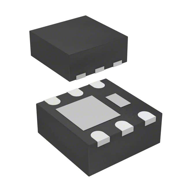
The FDMA1032CZ is MOSFET N/P-CH 20V MICROFET 2X2, that includes PowerTrenchR Series, they are designed to operate with a Digi-ReelR Alternate Packaging Packaging, Unit Weight is shown on datasheet note for use in a 0.001411 oz, that offers Mounting Style features such as SMD/SMT, Package Case is designed to work in 6-WDFN Exposed Pad, as well as the Si Technology, it has an Operating Temperature range of -55°C ~ 150°C (TJ). In addition, the Mounting Type is Surface Mount, the device is offered in 2 Channel Number of Channels, the device has a 6-MicroFET (2x2) of Supplier Device Package, and Configuration is N-Channel P-Channel, and the FET Type is N and P-Channel, and Power Max is 700mW, and the Transistor Type is 1 N-Channel 1 P-Channel, and Drain to Source Voltage Vdss is 20V, and the Input Capacitance Ciss Vds is 340pF @ 10V, and FET Feature is Logic Level Gate, and the Current Continuous Drain Id 25°C is 3.7A, 3.1A, and Rds On Max Id Vgs is 68 mOhm @ 3.7A, 4.5V, and the Vgs th Max Id is 1.5V @ 250μA, and Gate Charge Qg Vgs is 6nC @ 4.5V, and the Pd Power Dissipation is 1.4 W, it has an Maximum Operating Temperature range of + 150 C, it has an Minimum Operating Temperature range of - 55 C, and Fall Time is 8 ns 11 ns, and the Rise Time is 8 ns 11 ns, and Vgs Gate Source Voltage is 12 V, and the Id Continuous Drain Current is 3.7 A, and Vds Drain Source Breakdown Voltage is 20 V, and the Rds On Drain Source Resistance is 37 mOhms, and Transistor Polarity is N-Channel P-Channel, and the Typical Turn Off Delay Time is 14 ns 37 ns, and Typical Turn On Delay Time is 8 ns 13 ns, and the Forward Transconductance Min is 16 S - 11 S, and Channel Mode is Enhancement.
FDMA1028NZ_F021 with circuit diagram, that includes 3.7A Current Continuous Drain Id 25°C, they are designed to operate with a 20V Drain to Source Voltage Vdss, FET Feature is shown on datasheet note for use in a Logic Level Gate, that offers FET Type features such as 2 N-Channel (Dual), Gate Charge Qg Vgs is designed to work in 6nC @ 4.5V, as well as the 340pF @ 10V Input Capacitance Ciss Vds, the device can also be used as Surface Mount Mounting Type. In addition, the Mounting Style is SMD/SMT, the device is offered in 2 Channel Number of Channels, it has an Operating Temperature range of -55°C ~ 150°C (TJ), and Package Case is 6-WDFN Exposed Pad, and the Packaging is Digi-ReelR Alternate Packaging, and Power Max is 700mW, and the Rds On Drain Source Resistance is 3.9 mOhms, and Rds On Max Id Vgs is 68 mOhm @ 3.7A, 4.5V, and the Series is PowerTrenchR, and Supplier Device Package is MicroFET 2x2, and the Technology is Si, and Transistor Polarity is N-Channel, and the Transistor Type is 2 N-Channel, and Unit Weight is 0.002116 oz, and the Vds Drain Source Breakdown Voltage is 20 V, and Vgs th Max Id is 1.5V @ 250μA.
Features
PowerTrench® SeriesLow profile (maximum 0.8 mm) in the new MicroFET 2x2 package
RoHS Compliant; HBM ESD protection level > 2 kV usual (Note 3).
Applications
Switching applications
运输
包装


相似产品


产品属性
全选
型号系列: PowerTrench®
包装: 卷带(TR)
部件状态: 停产
晶体管类型: NPN,P 通道
使用案例: 负载开关
额定电压: 30V
额定电流(安培): 2.9A
安装类型: 表面贴装型
封装/外壳: 6-VDFN 裸露焊盘
供应商器件封装: 6-MicroFET(2x2)

onsemi
onsemi(前称ON Semiconductor)是一家全球领先的半导体供应商,致力于提供智能电源和传感技术。公司成立于1999年,总部位于美国亚利桑那州斯科茨代尔。onsemi的产品涵盖汽车、工业、电源管理和物联网等领域。


实时新闻


博斯克数字
收入: 85M
2022年的收入为8500万美元,与2021年增长63%。
国家: 105
博斯克服务全球105个国家的客户。
配件发货: 25M+
我们在过去的五年中发货了2.5亿个配件,比前五年增长148%。
制造商: 950
2022年,博斯克从近950个制造商售卖了配件。
热门产品
01 / 02
10

ACS712ELCTR-05B-T
Allegro MicroSystems
SENSOR CURRENT HALL 5A AC/DC

ACS758LCB-100B-PFF-T
Allegro MicroSystems
SENSOR CURRENT HALL 100A 5-CB

ACS758LCB-100U-PFF-T
Allegro MicroSystems
SENSOR CURRENT HALL 100A 5-CB

A1326LLHLT-T
Allegro MicroSystems
SENSOR HALL EFFECT ANALOG SOT23W

A3988SEVTR-T
Allegro MicroSystems
IC MTR DRVR BIPOLAR 3-5.5V 36QFN

A3906SESTR-T
Allegro MicroSystems
IC MTR DRVR BIPOLAR 2.5-9V 20QFN

A4982SLPTR-T
Allegro MicroSystems
IC MTR DRV BIPOLR 3-5.5V 24TSSOP

ACS713ELCTR-30A-T
Allegro MicroSystems
SENSOR CURRENT HALL 30A DC

A4989SLDTR-T
Allegro MicroSystems
IC MTR DRV BIPOLR 3-5.5V 38TSSOP

A3938SLDTR-T
Allegro MicroSystems
IC MOTOR DRIVER 18V-50V 38TSSOP