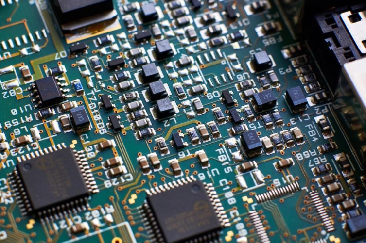
¥1545.60
价格更新:一个月前博斯克质量保证


Overview
The Cyclone II device family offers the following features:
● 133-MHz PCI-X 1.0 specification compatibility ● High-speed external memory support, including DDR, DDR2, and SDR SDRAM, and QDRII SRAM supported by drop in Altera IP MegaCore functions for ease of use ● Three dedicated registers per I/O element (IOE): one input register, one output register, and one output-enable register ● Programmable bus-hold feature ● Programmable output drive strength feature ● Programmable delays from the pin to the IOE or logic array ● I/O bank grouping for unique VCCIO and/or VREF bank settings ● MultiVolt™ I/O standard support for 1.5-, 1.8-, 2.5-, and 3.3-interfaces ● Hot-socketing operation support ● Tri-state with weak pull-up on I/O pins before and during configuration ● Programmable open-drain outputs ● Series on-chip termination support ■ Flexible clock management circuitry ● Hierarchical clock network for up to 402.5-MHz performance ● Up to four PLLs per device provide clock multiplication and division, phase shifting, programmable duty cycle, and external clock outputs, allowing system-level clock management and skew control ● Up to 16 global clock lines in the global clock network that drive throughout the entire device ■ Device configuration ● Fast serial configuration allows configuration times less than 100 ms ● Decompression feature allows for smaller programming file storage and faster configuration times ● Supports multiple configuration modes: active serial, passive serial, and JTAG-based configuration ● Supports configuration through low-cost serial configuration devices ● Device configuration supports multiple voltages (either 3.3, 2.5, or 1.8 V) ■ Intellectual property ● Altera megafunction and Altera MegaCore function support, and Altera Megafunctions Partners Program (AMPPSM) megafunction support, for a wide range of embedded processors, on-chip and off-chip interfaces, peripheral functions, DSP functions, and communications functions and protocols. Visit the Altera IPMegaStore at www.altera.com to download IP MegaCore functions. ● Nios II Embedded Processor support Functional Description Cyclone® II devices contain a two-dimensional row- and column-based architecture to implement custom logic. Column and row interconnects of varying speeds provide signal interconnects between logic array blocks (LABs), embedded memory blocks, and embedded multipliers. The logic array consists of LABs, with 16 logic elements (LEs) in each LAB. An LE is a small unit of logic providing efficient implementation of user logic functions. LABs are grouped into rows and columns across the device. Cyclone II devices range in density from 4,608 to 68,416 LEs. Cyclone II devices provide a global clock network and up to four phase-locked loops (PLLs). The global clock network consists of up to 16 global clock lines that drive throughout the entire device. The global clock network can provide clocks for all resources within the device, such as input/output elements (IOEs), LEs, embedded multipliers, and embedded memory blocks. The global clock lines can also be used for other high fan-out signals. Cyclone II PLLs provide general-purpose clocking with clock synthesis and phase shifting as well as external outputs for high-speed differential I/O support. M4K memory blocks are true dual-port memory blocks with 4K bits of memory plus parity (4,608 bits). These blocks provide dedicated true dual-port, simple dual-port, or single-port memory up to 36-bits wide at up to 260 MHz. These blocks are arranged in columns across the device in between certain LABs. Cyclone II devices offer between 119 to 1,152 Kbits of embedded memory Each embedded multiplier block can implement up to either two 9 × 9-bit multipliers, or one 18 × 18-bit multiplier with up to 250-MHz performance. Embedded multipliers are arranged in columns across the device Each Cyclone II device I/O pin is fed by an IOE located at the ends of LAB rows and columns around the periphery of the device. I/O pins support various single-ended and differential I/O standards, such as the 66- and 33-MHz, 64- and 32-bit PCI standard, PCI-X, and the LVDS I/O standard at a maximum data rate of 805 megabits per second (Mbps) for inputs and 640 Mbps for outputs. Each IOE contains a bidirectional I/O buffer and three registers for registering input, output, and output-enable signals. Dual-purpose DQS, DQ, and DM pins along with delay chains (used to phase-align double data rate (DDR) signals) provide interface support for external memory devices such as DDR, DDR2, and single data rate (SDR) SDRAM, and QDRII SRAM devices at up to 167 MHz.
Features
Cyclone® II Series422 I/Os
Up to 1152000 RAM bits
0°C ~ 85°C (TJ) Operating Temperature
Applications
There are a lot of Intel
EP2C70F672C6N FPGAs applications.
- Integrating multiple SPLDs
- Voice recognition
- Cryptography
- Filtering and communication encoding
- Aerospace and Defense
- Medical Electronics
- Audio
- Automotive
- Consumer Electronics
- Distributed Monetary Systems
- 起步价为$40,南非、巴西、印度、巴基斯坦、以色列等国家的价格会有所变动,详情请咨询相关客服人员。
- 包裹重量≤0.5kg的基本运费根据时区和国家而定。
- 我们的产品目前使用DHL,顺丰和UPS运输。如果数量少,则选择联邦快递。
- 一旦发货,预期交货时间跟选择的运输方式有所变动。
准备产品
真空包装
防静电袋
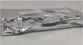
单独包装
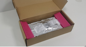
包装盒
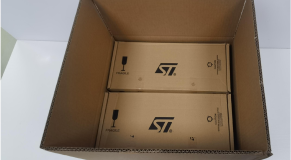
条形码运输标签
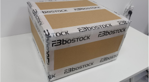

Altera
Altera公司是一家专注于开发和生产现场可编程门阵列(FPGA)的全球领先企业。成立于1983年,总部位于美国加利福尼亚州圣何塞。Altera的FPGA产品广泛应用于通信、数据中心、工业、汽车和军事航空等领域。2015年,Altera被英特尔公司收购,并于2024年重新独立运营,致力于推动FPGA市场的创新和增长。
热门零件号
实时新闻
博斯克数字
收入: 85M
2022年的收入为8500万美元,与2021年增长63%。
国家: 105
博斯克服务全球105个国家的客户。
配件发货: 25M+
我们在过去的五年中发货了2.5亿个配件,比前五年增长148%。
制造商: 950
2022年,博斯克从近950个制造商售卖了配件。
热门产品

ACS758LCB-100U-PFF-T
Allegro MicroSystems
SENSOR CURRENT HALL 100A 5-CB

A1326LLHLT-T
Allegro MicroSystems
SENSOR HALL EFFECT ANALOG SOT23W

A3988SEVTR-T
Allegro MicroSystems
IC MTR DRVR BIPOLAR 3-5.5V 36QFN

A4982SLPTR-T
Allegro MicroSystems
IC MTR DRV BIPOLR 3-5.5V 24TSSOP

A4989SLDTR-T
Allegro MicroSystems
IC MTR DRV BIPOLR 3-5.5V 38TSSOP

ACS713ELCTR-30A-T
Allegro MicroSystems
SENSOR CURRENT HALL 30A DC

A3906SESTR-T
Allegro MicroSystems
IC MTR DRVR BIPOLAR 2.5-9V 20QFN

ACS712ELCTR-05B-T
Allegro MicroSystems
SENSOR CURRENT HALL 5A AC/DC

ACS758LCB-100B-PFF-T
Allegro MicroSystems
SENSOR CURRENT HALL 100A 5-CB

A3938SLDTR-T
Allegro MicroSystems
IC MOTOR DRIVER 18V-50V 38TSSOP


