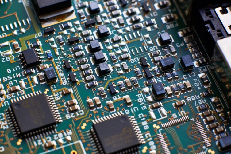
Cypress CY7C13121KV18-300BZXC
1M x 180°C ~ 70°C(TA)
比较


¥274.37
价格更新:一个月前博斯克质量保证


Overview
The CY7C13101KV18, CY7C13251KV18, CY7C13121KV18, and CY7C13141KV18 are 1.8 V Synchronous Pipelined SRAMs, equipped with QDR II architecture. QDR II architecture consists of two separate ports: the read port and the write port to access the memory array. The read port has dedicated data outputs to support read operations and the write port has dedicated data inputs to support write operations. QDR II architecture has separate data inputs and data outputs to completely eliminate the need to “turnaround” the data bus that exists with common I/O devices. Access to each port is through a common address bus. Addresses for read and write addresses are latched on alternate rising edges of the input (K) clock. Accesses to the QDR II read and write ports are completely independent of one another. To maximize data throughput, both read and write ports are equipped with DDR interfaces. Each address location is associated with two 8-bit words (CY7C13101KV18), 9-bit words (CY7C13251KV18), 18-bit words (CY7C13121KV18), or 36-bit words (CY7C13141KV18) that burst sequentially into or out of the device. Because data can be transferred into and out of the device on every rising edge of both input clocks (K and K and C and C), memory bandwidth is maximized while simplifying system design by eliminating bus turnarounds. Depth expansion is accomplished with port selects, which enables each port to operate independently. All synchronous inputs pass through input registers controlled by the K or K input clocks. All data outputs pass through output registers controlled by the C or C (or K or K in a single clock domain) input clocks. Writes are conducted with on-chip synchronous self-timed write circuitry. These devices are down bonded from the 65 nm 72M QDRII+/DDRII+ devices and hence have the same IDD/ISB1 values and the same JTAG ID code as the equivalent 72M device options. For details refer to the application note AN53189, 65 nm Technology Interim QDRII+/DDRII+ SRAM device family description.
• True Dual-Ported memory cells which allow simultaneous reads of the same memory location • 1K x 8 organization • 0.65-micron CMOS for optimum speed/power • High-speed access: 15 ns • Low operating power: ICC = 110 mA (max.) • Fully asynchronous operation • Automatic power-down • Master CY7C130/CY7C131 easily expands data bus width to 16 or more bits using slave CY7C140/CY7C141 • BUSY output flag on CY7C130/CY7C131; BUSY input on CY7C140/CY7C141 • INT flag for port-to-port communication • Available in 48-pin DIP (CY7C130/140), 52-pin PLCC, 52-Pin TQFP. • Pb-Free packages available
Features
Volatile Memory TypePackage / Case: 165-LBGA
165 Pins
Operating Supply Voltage:1.8V
I/O Type: SEPARATE
Surface Mount Mounting Type
Applications
There are a lot of Cypress Semiconductor Corp
CY7C13121KV18-300BZXC Memory applications.
- multimedia computers
- networking
- personal computers
- servers
- supercomputers
- telecommunications
- workstations,
- DVD disk buffer
- data buffer
- nonvolatile BIOS memory
- 起步价为$40,南非、巴西、印度、巴基斯坦、以色列等国家的价格会有所变动,详情请咨询相关客服人员。
- 包裹重量≤0.5kg的基本运费根据时区和国家而定。
- 我们的产品目前使用DHL,顺丰和UPS运输。如果数量少,则选择联邦快递。
- 一旦发货,预期交货时间跟选择的运输方式有所变动。
准备产品
真空包装
防静电袋
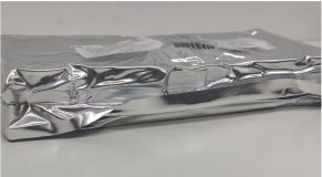
单独包装
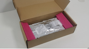
包装盒
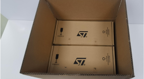
条形码运输标签
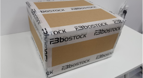

Cypress Semiconductor Corp
Cypress Semiconductor是一家知名的半导体公司,专注于高性能嵌入式系统解决方案。公司成立于1982年,总部位于美国加利福尼亚州圣何塞。Cypress的产品广泛应用于汽车、工业、消费电子和物联网市场。
实时新闻
博斯克数字
收入: 85M
2022年的收入为8500万美元,与2021年增长63%。
国家: 105
博斯克服务全球105个国家的客户。
配件发货: 25M+
我们在过去的五年中发货了2.5亿个配件,比前五年增长148%。
制造商: 950
2022年,博斯克从近950个制造商售卖了配件。
热门产品

A3906SESTR-T
Allegro MicroSystems
IC MTR DRVR BIPOLAR 2.5-9V 20QFN

A4982SLPTR-T
Allegro MicroSystems
IC MTR DRV BIPOLR 3-5.5V 24TSSOP

ACS758LCB-100U-PFF-T
Allegro MicroSystems
SENSOR CURRENT HALL 100A 5-CB

A3988SEVTR-T
Allegro MicroSystems
IC MTR DRVR BIPOLAR 3-5.5V 36QFN

ACS713ELCTR-30A-T
Allegro MicroSystems
SENSOR CURRENT HALL 30A DC

A4989SLDTR-T
Allegro MicroSystems
IC MTR DRV BIPOLR 3-5.5V 38TSSOP

A3938SLDTR-T
Allegro MicroSystems
IC MOTOR DRIVER 18V-50V 38TSSOP

A1326LLHLT-T
Allegro MicroSystems
SENSOR HALL EFFECT ANALOG SOT23W

ACS758LCB-100B-PFF-T
Allegro MicroSystems
SENSOR CURRENT HALL 100A 5-CB

ACS712ELCTR-05B-T
Allegro MicroSystems
SENSOR CURRENT HALL 5A AC/DC


